The process and materials used in Semiconductor manufacturing require high precision and wear resistance, as such the process of manufacturing these tools requires the most precise and resilient micro tools, making the process costly and complex, Telcon in this article reviews the place of Micro PCD Drills in Semiconductors Industry and main wear elements in the Semiconductor manufacturing process and shows how using the right tools for the job, can save both time and money for the manufacturer and of the Semiconductor Showerhead and of wafer holders in the Etching process using Telcon high precision micro PCD tools.
The Nature of Machining ceramic materials
Semiconductor manufacturers use ceramics for their mechanical and environmental stability in highly harsh and corrosive environments. Ceramics are adopted in packaging, where hermeticity, thermal conductivity, and mechanical integrity are highly needed. In communications and sensing, ceramic dielectrics support high rates of data transmission and monitoring. One of the vastly used semiconductors materials is Silicon.
Typical materials in Semiconductor industry
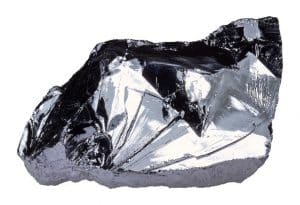
One of the most used materials in semiconductors is Monocrystalline silicon (c-Si). It has a crystalline structure, or crystal lattice, as continuous solid with no grain boundaries and with no impurities. It is the material for both silicon wafers and semiconductor processing components to avoid contamination. In addition, this gives monocrystalline silicon an advantage over other materials to reliably deliver desired performance specifications within highly complex devices such as microprocessors, electrodes, gas distribution plates. It can be doped with small amounts of other chemical elements to gain specific semiconductor performance characteristics.
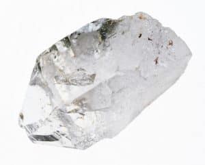
Another typical material in the semiconductors is Quartz or Fused Silica (SiO2). Its high heat resistance and purity allows the usage of quartz in silicon wafer manufacturing processes. Fused quartz plates and discs are needed in the semiconductor industry for the fabrication of boats, pedestals, wafers and wafer carriers, for batch processing equipment .For single wafer processing equipment, plates are used to make windows, gas distribution plates, shower plates, wafer carriers and susceptors. In wet cleaning processes the material is used for tank material. Large plates are also used in Flat panel display manufacturing.
Machining methods for Semiconductor industry materials
Most of semiconductor materials are difficult to machine because of their high hardness and brittleness. For example, monocrystalline silicone hardness is around 1200 Hv, Quartz hardness is around 1100 Hv, Alumina (Al2O3) hardness is 1500 Hv and SiC hardness is 2400 Hv. The limitations of mechanical micromachining in the mentioned materials are a consequence of the high values of cutting forces in relation to the tool strength properties, rapid cutting edges wear, chipping at the hole entry and possible cracks in the workpiece.
Micro holes with diameters below 1000 microns are a typical feature of various semiconductors components. There are few methods for micro drilling in hard ceramics; Laser drilling, EDM drilling and Mechanical drilling. Laser drilling would be effective from 5 to 100 microns. EDM micro drilling would be used in cases where very high ratio of hole depth to hole diameter is required given the workpiece material is conductive. Hole diameters from 300 microns and ratio depth of up to 30, are better mechanically drilled since it is faster and more accurate, therefore it is highly in use for semiconductors components.
Cutting tools solutions – Micro PCD Drills in Semiconductors Industry
Tungsten carbide tools are just too close in hardness to the workpiece materials, therefore wear out immediately. Due to the abrasiveness structure of these materials, also CVD diamond coated tools are not recommended due to rapid peel-off of the coating. Due to material properties as mentioned, machining process can only be made with PCD (Poly Crystalline Diamond) cutting tools. making Micro PCD Drills in Semiconductors Industry the only viable option.
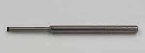
Telcon Diamond Ltd. is one of very small group of tool manufacturers to produce micro PCD tools for the semiconductors industry. There are two groups of tools: Micro PCD drills and Micro PCD end-mills. The machining is carried out utilizing highly sophisticated technology to achieve very accurate and ultrafine cutting edge. The PCD grade in use is suitable for micro tools with ultrafine tool edge integrity. Unlike other PCD cutting tools, these micro PCD tool are featured with full PCD head, whereas tool geometry can be fully flexible and optimized.
Telcon’s micro PCD drills series, MPDR, ranging from 0.4mm up to 2.0mm, are used for instance in semiconductors for drilling very tough materials like monocrystalline silicone and Quartz. The high-performance drills allow drilling thousands of holes before replacement.
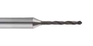
The micro PCD end-mills, ball nose (MPBN) and square end (MPEM) design, ranging from 0.5mm to 2.0mm, are used for machining of hard ceramic materials which are common in the semiconductors such as
Zirconia, Quartz, c-Si, Al2O3 and SiC.

Application Example 1 – practical use of Micro PCD Drills in Semiconductors Industry:
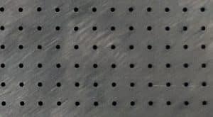
Drilling in c-Si wafer, 300mm diameter and 10mm thickness, 800 holes with diameter of 0.45mm and 7mm depth.
The part is a Gas Distributor Plate, used in the etching process of the silicon wafer.
Drill is used in 15,000 RPM and feed rate of 20 mm/min, in pecking cycle of 0.15mm.
The holes are inspected mainly for chipping at the hole entrance.
Typical Telcon drill life is 7000 good holes!
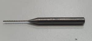
Typical hole structure on monocrystal silicon electrode. Holes: 0.45mm dia. x 7mm depth


Application Example 2:
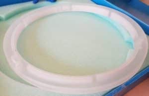
Machining of 25mm groove depth in Fused Silica (Quartz) material with 2.0mm micro PCD end mill.
The part is used as a carrier in the various processes of the silicon wafer.
The tool is used in 5,000 RPM and feed rate of 150 mm/min, in a depth of cut 0.05-0.1mm.
The material is inspected for chipping and small cracks.
Typical Telcon tool life is 50 meters minimum.
A typical Quartz ring, 300mm diameter, with internal grooves of 2.0mm width and 25mm depth.

For more information on our Micro tools solutions:
